本文利用等离子体辅助分子束外延(PA-MBE)系统, 对常规连续外延生长和金属调制外延(MME)生长AlN薄膜进行研究。研究发现: 常规连续外延方法生长模式不易控制, 容易出现过度富Al和富N模式生长, 而且微富Al模式生长还会出现一些凹坑, 表面形貌较粗糙; 然而利用MME方法生长AlN薄膜, 通过精准调控Al源和N源快门打开、关闭时间, 可以获得形貌较好的AlN薄膜。通过调整优化获得的MME方案为: 首先Al源快门打开30 s, 然后Al源和N源快门打开60 s, 最后单独打开N源快门72 s; 单一周期内, Al源快门打开时间与N源快门打开时间比例为0.7。以上述方案为一个周期进行循环生长40个周期, 可获得粗糙度低至0.3 nm(2 μm×2 μm), 几乎无凹坑的AlN薄膜。
金属调制 分子束外延 外延生长 氮化铝 粗糙度 metal modulation molecular beam epitaxy epitaxial growth aluminum nitride roughness
实现电学性能优良的高Al组分AlGaN外延层是制备深紫外光电器件最重要的环节之一。本工作利用分子束外延(MBE)技术, 基于周期热脱附的生长方式, 通过改变Al源供应量调控Al组分, 并用Si进行n型掺杂, 在AlN/蓝宝石衬底上得到了系列高Al组分的Si-AlxGa1-xN外延层(x>0.60)。对外延层相关物理性质进行了表征测试, 结果表明, 外延层Al组分与生长过程中Al束流大小呈现线性关系, 这为制备精确Al组分的AlGaN外延层奠定了基础。AFM结果表明, 高Al组分AlGaN外延层的表面形貌强烈依赖于Ga的供应量, 在生长过程中提高Ga束流可以显著降低外延层的粗糙度。基于范德堡法测量Si-AlGaN外延层电学性能, 证实其载流子特性良好, 其中 Al组分为0.93的样品室温下自由电子浓度、电子迁移率和电阻率分别达到了8.9×1018 cm-3和3.8 cm2·V-1·s-1和0.18 Ω·cm。
高Al组分AlGaN 分子束外延 Si掺杂 载流子特性 周期热脱附 high Al-content AlGaN molecular beam epitaxy Si doping carrier property periodic thermal desorption

Author Affiliations
Abstract
1 Nanjing University of Posts and Telecommunications, College of Electronic and Optical Engineering & College of Flexible Electronics (Future Technology), Nanjing, China
2 Nanjing University, School of Electronic Science and Engineering, Nanjing, China
The AlGaN/GaN p–n junction has received extensive attention due to its capability of rapid photogenerated carrier separation in photodetection devices. The AlGaN/GaN heterojunction nanowires (NWs) have been especially endowed with new life for distinctive transport characteristics in the photoelectrochemical (PEC) detection field. A self-powered PEC ultraviolet photodetector (PEC UV PD) based on the p-AlGaN/n-GaN heterojunction NW is reported in this work. The n-GaN NW layer plays a crucial role as a current flow hub to regulate carrier transport, which mainly acts as a light absorber under 365 nm and carrier recombination layer under 255 nm illumination, which can effectively modulate photoresponsivity at different wavelengths. Furthermore, by designing the thicknesses of the NW layer, the photocurrent polarity reversal was successfully achieved in the constructed AlGaN/GaN NW PEC UV PD at two different light wavelengths. In addition, by combining with platinum decoration, the photoresponse performance could be further enhanced. Our work provides insight into transport mechanisms in the AlGaN/GaN NW PEC system, and offers a feasible and comprehensive strategy for further exploration of multifunctional optoelectronic devices.
GaN nanowires ultraviolet detection photoelectrochemistry photoresponse Advanced Photonics Nexus
2023, 2(3): 036003

Author Affiliations
Abstract
1 Jiangsu Provincial Key Laboratory of Advanced Photonic and Electronic Materials, School of Electronic Science and Engineering, Nanjing University, Nanjing 210093, China
2 Xiamen University, Xiamen 361005, China
3 e-mail: bliu@nju.edu.cn
4 e-mail: rzhangxmu@xmu.edu.cn
We fabricated p-i-n tunnel junction (TJ) contacts for hole injection on c-plane green micro-light-emitting diodes (micro-LEDs) by a hybrid growth approach using plasma-assisted molecular beam epitaxy (PA-MBE) and metal–organic chemical vapor deposition (MOCVD). The TJ was formed by an MBE-grown ultra-thin unintentionally doped InGaN polarization layer and an layer on the activated layer prepared by MOCVD. This hybrid growth approach allowed for the realization of a steep doping interface and ultrathin depletion width for efficient inter-band tunneling. Compared to standard micro-LEDs, the TJ micro-LEDs showed a reduced device resistance, enhanced electroluminescence intensity, and a reduced efficiency droop. The size-independent J-V characteristics indicate that TJ could serve as an excellent current spreading layer. All these results demonstrated that hybrid TJ contacts contributed to the realization of high-performance micro-LEDs with long emission wavelengths.
Photonics Research
2021, 9(9): 09001683
Author Affiliations
Abstract
1 School of Electronic Science and Engineering, Collaborative Innovation Center of Advanced Microstructures, Nanjing University, Nanjing 210023, China
2 School of Electronic and Information Engineering, Nanjing University of Information Science & Technology Binjiang College, Wuxi 214105, China
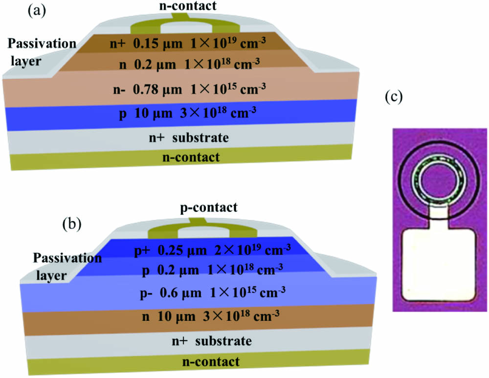
Understanding detailed avalanche mechanisms is critical for design optimization of avalanche photodiodes (APDs). In this work, avalanche characteristics and single photon counting performance of 4H-SiC n-i-p and p-i-n APDs are compared. By studying the evolution of breakdown voltage as a function of incident light wavelength, it is confirmed that at the deep ultraviolet (UV) wavelength region the avalanche events in 4H-SiC n-i-p APDs are mainly induced by hole-initiated ionization, while electron-initiated ionization is the main cause of avalanche breakdown in 4H-SiC p-i-n APDs. Meanwhile, at the same dark count rate, the single photon counting efficiency of n-i-p APDs is considerably higher than that of p-i-n APDs. The higher performance of n-i-p APDs can be explained by the larger impact ionization coefficient of holes in 4H-SiC. In addition, this is the first time, to the best of our knowledge, to report single photon detection performance of vertical 4H-SiC n-i-p-n APDs.
4H-SiC avalanche photodiode electron-initiated ionization hole-initiated ionization Chinese Optics Letters
2021, 19(9): 092501

Author Affiliations
Abstract
1 School of Electronic Science and Engineering, Nanjing University, Nanjing 210023, China
2 e-mail: wz.xu@nju.edu.cn
3 e-mail: hailu@nju.edu.cn
In this work, a GaN p-i-n diode based on Mg ion implantation for visible-blind UV detection is demonstrated. With an optimized implantation and annealing process, a p-GaN layer and corresponding GaN p-i-n photodiode are achieved via Mg implantation. As revealed in the UV detection characterizations, these diodes exhibit a sharp wavelength cutoff at 365 nm, high UV/visible rejection ratio of 1.2×10⁴, and high photoresponsivity of 0.35 A/W, and are proved to be comparable with commercially available GaN p-n photodiodes. Additionally, a localized states-related gain mechanism is systematically investigated, and a relevant physics model of electric-field-assisted photocarrier hopping is proposed. The demonstrated Mg ion-implantation-based approach is believed to be an applicable and CMOS-process-compatible technology for GaN-based p-i-n photodiodes.
Photonics Research
2019, 7(8): 08000B48
1 School of Electronic and Electrical Engineering, Chuzhou University, Chuzhou 239000, China
2 Key Laboratory of Advanced Photonic and Electronic Materials, School of Electronic Science and Engineering, Nanjing University, Nanjing 210093, China
3 College of Physics and Electronic Information, Anhui Normal University, Wuhu 241000, China
Jiangsu Provincial Key Laboratory of Advanced Photonic and Electronic Materials, Department of Physics, Nanjing University, Nanjing 210093, China
Frontiers of Optoelectronics
2009, 2(4): 442


